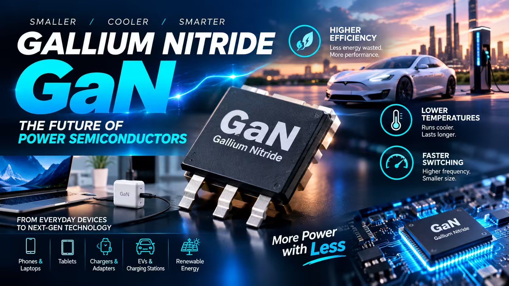
Gallium Nitride (GaN) has moved from a laboratory curiosity to the foundational technology of modern power electronics. With a bandgap of 3.4 eV and a critical electric field ten times that of silicon, GaN enables chargers that are half the size, data centers that waste less energy, and electric vehicles that charge faster. This guide covers the physics, the applications, and the market.
This article provides a comprehensive analysis of Gallium Nitride (GaN) technology as it stands in 2026. It examines the fundamental material properties that give GaN its advantages over silicon, explores the two main device architectures (enhancement-mode and cascode), and reviews the major application areas including fast chargers, data centers, electric vehicles, and renewable energy. The guide also covers the current market landscape, key manufacturers, and the challenges that remain for widespread adoption. The goal is to provide a complete reference for engineers, product managers, and technology enthusiasts seeking to understand this transformative semiconductor technology.
What is Gallium Nitride? The Physics Behind the Hype
Gallium Nitride (GaN) is a wide-bandgap semiconductor material that has emerged as the leading replacement for silicon in power electronics. Unlike silicon, which has a bandgap of 1.12 eV, GaN has a bandgap of 3.4 eV [citation:1]. This difference may seem small, but it fundamentally changes how the material behaves under electrical stress. The critical electric field of GaN is approximately 3.3–3.5 MV/cm, more than ten times silicon's ~0.3 MV/cm [citation:1].
This higher critical field strength drives several structural advantages. A GaN layer can be roughly 10–11 times thinner than silicon for the same blocking voltage. The thinner layer has lower resistivity, which reduces on-resistance (RDS(on)). A smaller die size results in lower parasitic capacitance, and lower capacitance directly reduces switching losses [citation:1]. The system-level result is the ability to switch efficiently at frequencies well above 1 MHz, enabling smaller magnetics and higher-power-density designs.
GaN is not mined; it is grown. Scientists use a process called Metalorganic Chemical Vapor Deposition (MOCVD). Gases containing gallium and nitrogen are pumped into a vacuum chamber heated to temperatures often exceeding 1,000°C. The gases react, causing atoms of gallium and nitrogen to arrange themselves into a perfectly flat, atom-thick crystal layer onto a base substrate, usually silicon or sapphire [citation:6].
The Two Architectures: Enhancement-Mode vs. Cascode
GaN transistors are fundamentally different from silicon MOSFETs in one critical way: they lack a reliable insulator technology. This complicates the design of devices that are "fail-safe"—in other words, that fail open if the control circuit fails [citation:11]. Manufacturers use two architectures to achieve the normally-off behavior that power systems require:
Enhancement-mode (e-mode) GaN uses a p-GaN gate structure to shift the threshold voltage positive, creating a normally-off device. The threshold voltage VGS(th) is very low — typically 1 to 2 V — making the device sensitive to unintended switch-on in high dv/dt applications, which makes gate driver design demanding [citation:1].
Cascode GaN co-packages a high-voltage d-mode GaN HEMT with a low-voltage silicon MOSFET to achieve enhancement-mode operation. This interface naturally isolates the device gate, offering an automotive-grade maximum gate rating of ±20 V, with exceptional reliability and a high drive margin [citation:1].
Neither approach is universally superior. E-mode devices offer a smaller footprint and tighter integration; cascode devices preserve the 2DEG in its natural, unmodified state and tolerate the same gate drive signals as a standard silicon MOSFET [citation:1].
GaN vs. Silicon: A Complete Comparison
The performance gap between GaN and silicon ultimately traces back to fundamental material properties. The table below summarizes the key differences [citation:1][citation:2].
| Parameter | Silicon (Si) | Gallium Nitride (GaN) | Practical Impact |
|---|---|---|---|
| Bandgap Energy (Eg) | 1.12 eV | 3.4 eV | Higher critical field; better high-temperature stability. |
| Critical Electric Field | ~0.3 MV/cm | ~3.3–3.5 MV/cm | Smaller die for the same blocking voltage; lower parasitics. |
| Electron Mobility (µ) | ~1,400 cm²/Vs | ~2,000 cm²/Vs (2DEG) | Lower RDS(on) for reduced conduction losses. |
| Reverse Recovery Charge (Qrr) | High (nC to µC) | 0 | Eliminates a primary switching loss mechanism. |
| Max Gate Voltage | ±20 V | −5 V to +6 V (e-mode) / ±20 V (cascode) | E-mode requires a precision gate driver; cascode does not. |
| Switching Frequency | Typically <200 kHz | MHz range | Smaller magnetics; higher power density. |
| Efficiency (Typical) | 85–90% | 95%+ | Less energy lost as heat; smaller thermal solutions. |
The second major structural advantage of GaN is the absence of a body diode. In a silicon MOSFET, reverse current flows through the intrinsic body diode, which stores the reverse recovery charge (Qrr). That charge must be removed on every switching cycle, and the energy is dissipated as heat. In contrast, e-mode GaN has zero Qrr and does not rely on a body diode. This eliminates reverse recovery losses entirely and makes GaN particularly well suited for hard-switching topologies, including half-bridges and totem-pole power factor correction (PFC) [citation:1].
Why GaN Matters: The Application Landscape
GaN's physical advantages reduce the energy stored per switching cycle proportionally with frequency. Switch faster, and the magnetics (transformers, inductors, filters) shrink accordingly. This system-level payoff has driven adoption across multiple industries.
Fast Chargers and Consumer Adapters
Consumer electronics were GaN's proving ground. Fast chargers have been among the earliest adopters, driving volume growth and ecosystem maturity. Today, 65 W to 140 W GaN-based USB-C adapters fit in a fraction of the volume of their silicon predecessors because MHz-range switching frequencies allow the passive filter components to be dramatically smaller [citation:1]. A 65W silicon charger typically exceeds 150 cm³ in volume, while an equivalent GaN charger can be compressed to under 60 cm³ [citation:12]. The weight difference is also significant: a 120W silicon gaming laptop charger weighs around 480g, while a GaN version weighs only 220g, a 60% reduction [citation:12].
GaN chargers operate at 95% efficiency compared to silicon's typical 85-90%, meaning less energy is lost as heat. This is why a very small charger with high power output is not a safety concern; it is simply more efficient [citation:7].
Data Centers and AI Servers
Server racks require maximum compute density with minimal power overhead. The industry's shift from 12 V to 48 V rack backplanes requires highly efficient point-of-load step-down conversion. Modern AI accelerators now reach thermal design powers above 1.4 kW, driving a transition to 48 V rack distribution to reduce supply current and thereby conduction losses and copper mass [citation:8]. With global data center electricity consumption already surpassing that of entire industrialized nations like Germany or France, there is an urgent need for 48 V DC-DC converters combining high efficiency with exceptional power density [citation:8].
GaN devices are enabling new benchmarks in this space. A 5 kW GaN-based AC-to-48 V DC reference design from EPC achieves up to 96.5% system efficiency and a combined power density of 116 W/in³, designed to meet Open Rack V3 (OCP ORv3) size requirements [citation:3]. A vertically integrated 3D "power brick" module using GaN FETs has achieved a 59.7% footprint reduction compared to an equivalent planar implementation, with a peak efficiency of 93.1% and power density of 2.15 kW/in³ [citation:8].
Regulatory pressure is also a factor. The U.S. Environmental Protection Agency is expanding ENERGY STAR initiatives to improve data center energy efficiency, including verification and rating of power supply efficiency. This is driving operators to adopt high-efficiency power units, increasing demand for GaN devices [citation:10].
Electric Vehicles (EVs)
GaN devices improve the efficiency of on-board chargers (OBCs) by 2 to 3 percentage points compared to silicon MOSFET-based designs and enable DC-DC converters that are 30 to 40% smaller in volume. This directly supports the automotive industry's transition to lighter, more integrated powertrain architectures. The commercial shift to 800 V platforms, exemplified by the Porsche Taycan, Hyundai IONIQ 5, and Kia EV6, extends GaN's addressable market beyond on-board chargers to auxiliary traction circuits and bidirectional vehicle-to-grid systems [citation:5].
GaN-based power devices, primarily GaN high-electron-mobility transistors (HEMTs), are increasingly adopted in low- to medium-voltage EV subsystems. GaN HEMTs exhibit extremely fast switching speeds, low gate charge, and minimal parasitic capacitances, making them ideal for high-frequency and high-efficiency power conversion. These properties are particularly advantageous for on-board chargers, auxiliary power supplies, and DC-DC converters operating below 650 V [citation:14].
Renewable Energy and Solar Inverters
Global solar PV capacity additions exceeded 400 GW in 2024, continuing a record installation pace that intensifies demand for high-efficiency inverter components capable of maintaining performance over 20- to 25-year project lifetimes. GaN-based inverters achieve switching efficiencies above 99% at partial load, a relevant improvement over IGBT alternatives in solar applications where partial-load operation represents the majority of annual operating hours. SolarEdge and SMA Solar have integrated GaN transistors into their residential and commercial string inverter platforms [citation:5].
The GaN Market in 2026: Growth and Key Players
The GaN power device market has experienced considerable growth. Between 2022 and 2024, the market grew from $211.1 million to $392.2 million. This growth was driven by the electrification of vehicle platforms, increasing energy efficiency requirements in digital infrastructure, and the rise of fast-charging consumer devices. Additional momentum came from pilot projects using GaN in high-voltage automotive systems and public investments supporting domestic wide-bandgap semiconductor ecosystems [citation:10].
The discrete GaN power transistor segment led the market with a 60.1% share in 2025, driven by their widespread adoption in consumer fast chargers, data center power supplies, and telecom power systems. These devices offer design flexibility, reduced system cost, and easier integration into existing power architectures, making them the preferred choice for high-volume, cost-sensitive applications [citation:10].
The smart GaN power module segment is expected to grow at a CAGR of 32.4% over the forecast period due to increasing demand from automotive, industrial, and aerospace applications. Integrated gate drivers, protection features, and enhanced packaging are driving this growth [citation:10].
Key Manufacturers and Ecosystem
The GaN ecosystem includes several major players. Infineon, EPC (Efficient Power Conversion), GaN Systems, Navitas Semiconductor, Power Integrations, Texas Instruments, and Transphorm are among the leading manufacturers of GaN power devices [citation:11]. The GaNFast technology platform from Navitas Semiconductor and the LMG3522R030-Q1 from Texas Instruments, an automotive-grade GaN FET, illustrate how adoption is broadening simultaneously in consumer and industrial supply chains, with GaN-based consumer charger unit shipments reaching tens of millions per year [citation:5].
Challenges and Limitations
Despite its advantages, GaN technology faces several challenges that limit its widespread adoption [citation:7]:
- Cost: GaN substrates are far more complex and expensive to fabricate than standard silicon wafers. Manufacturers must use sapphire, silicon carbide, or silicon wafers via chemical vapor deposition. This higher manufacturing cost translates to higher prices for consumers. A basic 5W to 15W silicon charger costs around $12, while a GaN charger starts at $30 [citation:7].
- Circuit Complexity: Because GaN passes energy more efficiently and creates less heat, it requires special internal circuit boards with specialized gate drivers, high-frequency transformers, and precise electromagnetic interference shielding to prevent electrical noise [citation:7].
- Limited Benefit for Low-Power Devices: For basic everyday devices that charge with 5W to 15W of power, there is no benefit to choosing a GaN charger. The technology only makes sense for demanding accessories like laptops, tablets, and the latest smartphones [citation:7].
- Reliability Concerns: Reliability issues related to GaN trap effects are still being studied. Dynamic on-resistance degradation, threshold voltage instability, and electromagnetic interference challenges remain areas of active research [citation:9].
Conclusion: The Future is Wide-Bandgap
GaN technology has transitioned from a promising laboratory material to a foundational technology of modern power electronics. Its superior material properties—wide bandgap, high critical electric field, high electron mobility, and zero reverse recovery charge—enable power systems that are smaller, more efficient, and more capable than anything possible with silicon.
In 2026, GaN is found in fast chargers that fit in a pocket, data center power supplies that approach 97% efficiency, and electric vehicle subsystems that reduce weight and extend range. The market is growing rapidly, driven by regulatory pressure for energy efficiency, the demands of AI infrastructure, and the electrification of transportation.
While challenges remain—particularly cost and the complexity of gate driver design—the trajectory is clear. As manufacturing scales and reliability data accumulates, GaN will continue to displace silicon in an ever-widening range of applications, from the charger in your bag to the power infrastructure of the world's largest data centers.
 Lorraine Hayes
Cloud Architect / Content Designer
eBits Tech Platform
@ eBits.icu