
The AMD Zen 5 microarchitecture represents the fifth generation of AMD's high-performance x86 core design, codenamed "Nirvana," and it marks a significant evolution in the company's processor technology. Launched in 2024, Zen 5 powers a wide array of products, including the Ryzen 9000 series desktop processors (codenamed "Granite Ridge"), the Ryzen AI 300 series mobile processors ("Strix Point"), and the EPYC 9005 server processors ("Turin") .
Built on TSMC's advanced 4nm FinFET process, Zen 5 delivers a reported 16% generational increase in instructions per clock (IPC) in desktop PC applications, a leap that combines architectural refinements with substantial new capabilities .
The Design Philosophy: Performance, Efficiency, and Balance
AMD's primary design objectives for Zen 5 were to deliver another major single-threaded (1T) and multi-threaded (NT) performance increase, balanced cross-core instruction and data throughput, and to provide support for AVX-512 and FP512 data paths for both general throughput and AI workloads . The architecture maintains the same basic structure as the previous Zen 4 generation, using a chiplet design with one or more CPU complex dies (CCDs) connected to a central I/O die (IOD) . However, the improvements are substantial, targeting front-end parallelism, execution parallelism, and efficient data movement .
Technical Specifications: The Core
Zen 5 is fabricated in TSMC's 4nm FinFET process, with the CCD being 55mm2 in size and containing 8.6 billion transistors across eight cores . The core complex (CCX) includes eight cores, each with a 1MB private L2 cache and a shared 32MB L3 cache . The I/O die (IOD) is built on a 6nm process and includes integrated RDNA 2 graphics with 128 stream processors, a PCI Express 5.0 controller, and a memory controller . The "Zen 5c" variant is designed for higher density and power efficiency in key markets .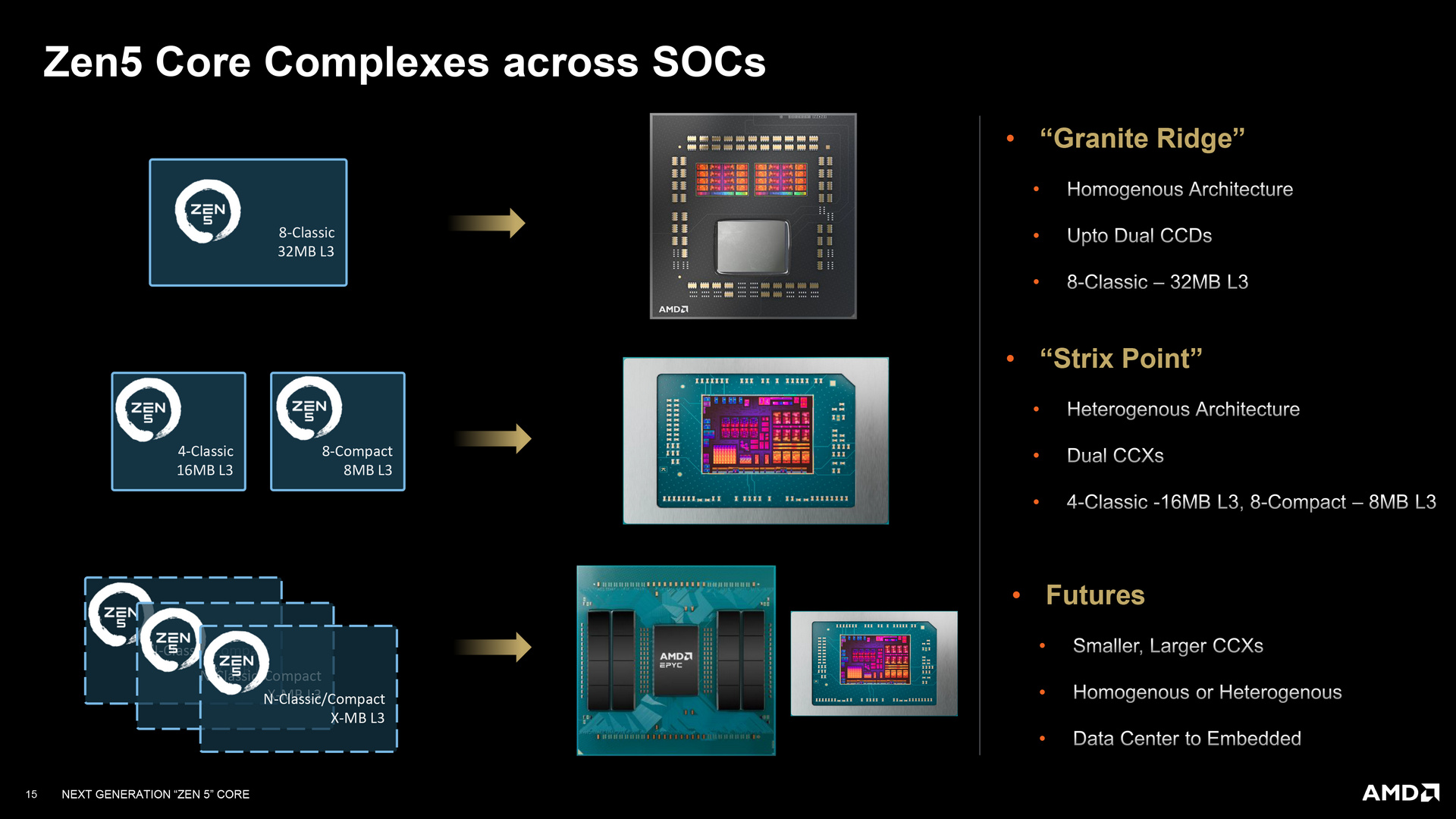
Core Architecture: Nirvana
The "Nirvana" core is the heart of the Zen 5 architecture, featuring several key improvements over its predecessor:
-
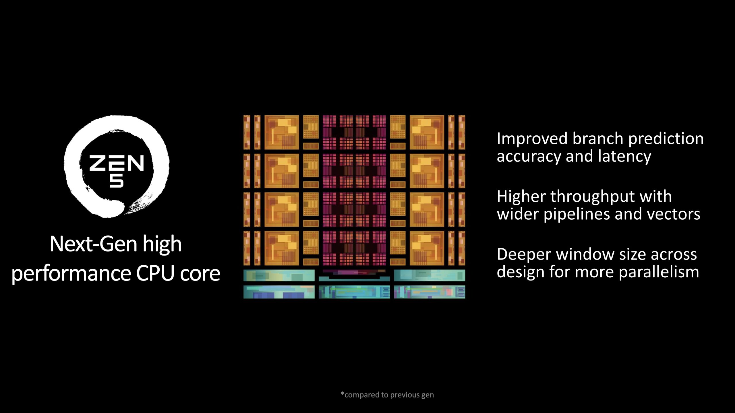
Front-End Enhancements: The front-end has been significantly expanded to improve instruction throughput and branch prediction accuracy. The instruction fetch rate has been increased from 16 bytes to 32 bytes per clock cycle, a change that addresses a long-standing bottleneck in both AMD and Intel processors . The branch predictor features zero-bubble conditional branches, a larger L2-sized L1 BTB, a larger return address stack, and the ability to make two taken predictions per cycle, which allows for fewer pipeline bubbles, increased accuracy, and higher throughput . The L1 instruction cache (I-Cache) is 32KB, 8-way, with a 2x32B fetch per cycle .
-
Decode and Dispatch: The decoders feature a dual decode pipe design that can handle two independent instruction streams or basic blocks in parallel, with a throughput of four instructions per cycle per pipe . The op-cache has 33% more entry associativity, offering increased density and coverage, and can output 12 instructions per cycle through two pipes . This feeds into an 8-wide dispatch that sends instructions to the integer or floating-point execution units .
-
Execution Engines: The execution capabilities of Zen 5 have been broadened substantially. The architecture features:
-
Integer: 6 integer ALUs and 4 AGU (address generation units) for memory operations, capable of executing up to six simple integer instructions per clock cycle .
-
Floating-Point Unit (FPU): The FPU is a major highlight, featuring full 512-bit AVX-512 data paths, a significant upgrade over Zen 4's implementation . It includes 4 execution pipes and can process vector additions and multiplications at a rate of two per cycle simultaneously . The latency for integer vector addition has increased from 1 to 2 cycles, while floating-point addition latency has been reduced from 3 to 2 cycles . This FPU is designed to double AI performance and AVX-512 throughput .
-
-
Memory Subsystem: The memory subsystem has also seen bandwidth improvements. The L1 data cache (D-Cache) is 48KB, 12-way, and can deliver four memory operations per cycle . The L2 cache has been upgraded from an 8-way to a 16-way associative design, effectively doubling its bandwidth . The data bandwidth between the L1, L2, and L3 caches has also been increased .

Product Codenames
The Zen 5 microarchitecture spans a wide range of products, from high-end servers to energy-efficient mobile processors.
-
Granite Ridge: The codename for the Ryzen 9000 series desktop processors. Built in the Socket AM5 package and drop-in compatible with all current AM5 motherboards with a BIOS update, the processors use a chiplet design with 4nm CCDs and a 6nm I/O die .
-
Strix Point: The codename for the Ryzen AI 300 series mobile processors. These are monolithic chips built on the 4nm node that combine "Zen 5" and "Zen 5c" cores for a maximum of 12 cores and 24 threads .
-
Turin: The codename for the EPYC 9005 server processors. These are high-end server multiprocessors that can scale up to 192 cores .
-
Shimada Peak: The codename for the Ryzen Threadripper 9000 workstation and enthusiast processors .
-
Fire Range: A high-performance mobile chip for gaming laptops .
 Performance Benchmarking and Comparisons
AMD's internal testing demonstrates the performance gains of the Zen 5 architecture. In a comparison between a Ryzen 9 9950X (Zen 5) and a Ryzen 7 7700X (Zen 4), the Zen 5 system showed significant performance uplifts in various applications, including Handbrake, League of Legends, FarCry 6, Puget Adobe Premiere Pro, 3DMark Physics, Kraken, Blender, Cinebench, Geekbench, Octane, Speedometer, and WebXPRT .
AMD claimed the Zen 5 core delivers a 16% generational IPC increase in desktop PC applications, an improvement that, while significant, is smaller than the 19% jump seen from Zen 2 to Zen 3 . However, it is a larger jump than the 14% seen from Zen 3 to Zen 4 . The architecture supports frequencies up to 5.7 GHz, matching the previous generation's peak speeds . AMD has also highlighted that Zen 5 chips can run cooler and consume lower power than their predecessors .
The Zen 5c Variant: Density and Efficiency
The Zen 5 family includes a "Zen 5c" variant, which is designed for increased density and power efficiency in key markets . This compact core is used in the "Strix Point" mobile processors alongside full-sized "Zen 5" cores to balance performance and efficiency . The Strix Point design features four "Zen 5" cores that can achieve the highest possible boost frequencies, and eight "Zen 5c" cores that feature an identical IPC and the full ISA but do not boost as high .
Cache and Bandwidth
The Zen 5 architecture features a redesigned cache structure that focuses on improving latency and bandwidth. The L2 cache has been doubled in bandwidth and uses a 16-way associative design . The L1 data cache now provides four memory operations per cycle . The FPU to L1 and L1 to L2 data bandwidth has been doubled . The L3 cache per CCD is 32 MB, which is consistent with the previous generation . The cache sizes have received only minor improvements, but the bandwidth and efficiency have been substantially increased .
AVX-512 Support and AI Capabilities
A key differentiator for Zen 5 is its robust support for AVX-512 instructions, with a full 512-bit FPU data path . This is a point of distinction from Intel's "Raptor Lake" and "Meteor Lake" processors, which do not support the instruction set, and "Arrow Lake," where its inclusion remains unclear . The FPU is designed to double the performance of AI and AVX-512 workloads, positioning Zen 5 as a strong option for emerging AI and machine learning tasks . The six pipelines in the FPU are capable of processing a floating-add (FADD) instruction in just two clock cycles, which is a significant improvement .
Conclusion
The AMD Zen 5 architecture is a significant step forward in the evolution of high-performance x86 processors. It combines a 4nm manufacturing process with major architectural enhancements to deliver a 16% IPC improvement. The architecture's strengths lie in its widened front-end, dual decode pipes, 8-wide dispatch, and a powerful FPU with full AVX-512 support. Its chiplet design maintains compatibility with existing AM5 motherboards, offering a straightforward upgrade path for desktop users. While the improvements are impressive, Zen 5 is not a revolution; it is a carefully engineered evolution that builds on the successes of its predecessors while introducing new capabilities for AI and high-performance computing. The architecture represents a balanced approach, targeting both performance and energy efficiency across a wide range of computing platforms.
 Claire Jones
Cloud Engineer / Technical Writer
eBits Tech Platform @ ebits.icu