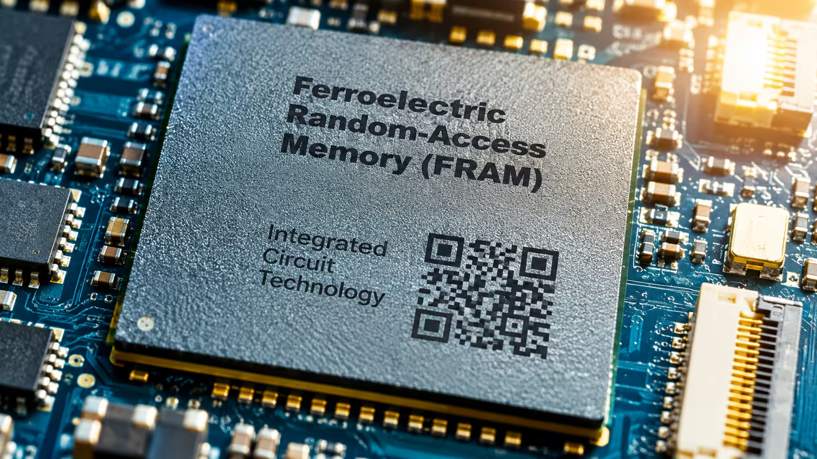
Ferroelectric RAM (FRAM) has long been positioned as a promising alternative to conventional memory, but 2026 marks a turning point. With a major density breakthrough at 22nm, near-DRAM speeds of 20–25 ns, and industrial integration by Fraunhofer and GlobalFoundries, FRAM is finally moving from laboratory curiosity toward commercial reality. This guide examines whether it can address the ongoing RAM crisis.
This article provides a comprehensive analysis of Ferroelectric RAM (FRAM) technology in 2026. It covers the fundamental architecture and physical principles that distinguish FRAM from DRAM and NAND flash, the breakthrough in 3D capacitor scaling achieved by CEA-Leti at the 22nm node, the industrial integration efforts led by Fraunhofer IPMS and GlobalFoundries, the performance characteristics including nanosecond write speeds and wide temperature operation, and the critical question of whether FRAM can alleviate the global memory shortage driven by AI demand. The goal is to offer a definitive reference for engineers, product managers, and technology professionals seeking to understand the current state and future potential of this emerging memory technology.
What Is FRAM? Architecture and Fundamental Principles
Ferroelectric Random Access Memory (FRAM) is a non-volatile memory technology that stores data through the spontaneous polarization of certain crystalline materials. Unlike DRAM, which relies on charge storage in capacitors that must be constantly refreshed, FRAM uses the position of atoms within a ferroelectric crystal lattice to represent binary states. When an electric field is applied, certain atoms shift between two stable positions, creating two distinct polarization orientations that correspond to the 0 and 1 states. These states persist indefinitely without power, in the same way a permanent magnet retains its magnetization without electricity [citation:13].
The standard FRAM cell architecture is 1T-1C, meaning one transistor and one capacitor. The transistor acts as a selector, while the ferroelectric capacitor stores the data bit. Historically, the planar capacitor structure limited cell density because the capacitor footprint, not the transistor, determined the cell size. The current flowing through the capacitor during read and write operations is inherently low, making the capacitor the dominant factor in cell area. This physical constraint kept FRAM confined to niche applications where its unique properties justified the cost premium [citation:5].
The 2026 Breakthrough: 3D Ferroelectric Capacitors at 22nm
In June 2026, researchers at CEA-Leti announced a major breakthrough that removes the density barrier that had held FRAM back for decades. By vertically integrating ferroelectric capacitors made from hafnium zirconium oxide (HZO) thin films, the team achieved memory cells that are 2.5 times smaller than standard SRAM at the same 22nm node, matching the density of SRAM at the much more advanced 10nm node. Unlike SRAM, however, FRAM retains data without power, combining non-volatility with a density previously attainable only by volatile memory [citation:1][citation:5].
The key innovation was shifting from a planar to a vertical architecture. Instead of building the capacitor outward across the wafer surface, the researchers built it upward, stacking it vertically. This approach maximizes the effective surface area of the ferroelectric capacitor within each bitcell, enlarging the memory window without sacrificing array density [citation:1].
The team demonstrated two back-end-of-line (BEOL) integration schemes for 3D ferroelectric capacitors at 22nm, using advanced patterning and deposition techniques. Array functionality with Gaussian bit distributions was confirmed down to 0.047 μm² 1T-1C FRAM bitcells operating at just 1.3V, featuring a standard logic selector and a 3D FeCap with an aspect ratio of roughly 4:1. The researchers also demonstrated a clear path to even greater density: 3D FeCaps with an aspect ratio of 17:1, a 60nm diameter, and a 120nm pitch, shrinking the capacitor footprint to just 0.0028 μm² [citation:5].
Performance Characteristics: Speed, Power, and Reliability
The performance characteristics of 2026-era FRAM are compelling, particularly for embedded and edge applications. A paper published in IEEE Transactions on Electron Devices in August 2026 demonstrated an HZO-based FRAM that achieves near-DRAM performance, featuring fast write/read speeds of 20–25 ns and low operating voltages of approximately 1.4 V across broad temperature conditions [citation:6][citation:8].
The fabricated arrays exhibited a 100% pass rate in long-term retention tests, confirming exceptional stability across a wide temperature range of -40°C to 175°C. This wide-temperature operation makes FRAM particularly attractive for automotive, industrial, and aerospace applications where conventional memory technologies struggle [citation:6].
A critical reliability challenge for ferroelectric memory has been the "wake-up" phenomenon, where electrical characteristics shift unpredictably during initial cycling, degrading stability. CEA-Leti's high-aspect-ratio 3D capacitors exhibited wake-up-free behavior, consistent with an approximately 80% orthorhombic phase fraction in the HZO film as confirmed by precession electron diffraction. The suppression of wake-up is likely related to the confinement of materials within the narrow, high-aspect-ratio vias, which locally modifies the strain state in the ferroelectric thin film and stabilizes the crystal phase responsible for memory function from the outset [citation:5].
Industrial Integration: From Research to Manufacturing
The transition from laboratory demonstration to industrial production is a critical milestone for any emerging memory technology. In 2026, this transition is actively underway. The Fraunhofer Institute for Photonic Microsystems IPMS, in collaboration with GlobalFoundries, has successfully integrated a reproducible approach for hafnium oxide-based ferroelectric FRAM memory into an existing industrial manufacturing technology [citation:12].
The work, which received the 2026 Stifterverband Science Prize, is based on systematic co-optimization of materials, layer stacks, processes, and modules. The jury highlighted "the qualitative leap beyond international standards" and the exemplary "cross-institutional collaboration to strengthen Germany as an industry hub." The technology enables especially compact, fast, and highly reliable data storage devices with low energy consumption and stable operation even under demanding conditions [citation:12].
A crucial advantage of this approach is that hafnium oxide is already part of modern semiconductor manufacturing processes. It does not require exotic materials or new infrastructure; it can be integrated into existing production lines. The collaboration between Fraunhofer IPMS and GlobalFoundries, developed within the Silicon Saxony ecosystem in Dresden, exemplifies the European strategy to reinforce its semiconductor capacity under initiatives like the European Chips Act [citation:13].
FRAM vs. DRAM vs. NAND: A Comparative Analysis
Understanding FRAM's position in the memory hierarchy requires comparing it directly with the dominant technologies. The following table summarizes the key differences based on 2026 specifications.
| Characteristic | FRAM | DRAM | NAND Flash |
|---|---|---|---|
| Volatility | Non-volatile | Volatile (requires refresh) | Non-volatile |
| Write Speed | 20–25 ns | ~10–20 ns | ~100 μs – 1 ms |
| Read Speed | 20–25 ns | ~10–20 ns | ~25–100 μs |
| Endurance | ~10¹²–10¹⁵ cycles | Unlimited (theoretically) | ~10³–10⁵ cycles |
| Write Energy | Very low (~1.4V) | Continuous refresh power | High (requires charge pump) |
| Density (2026) | 22nm (0.047 μm²) | 10nm-class (mature) | 3D stacking (mature) |
| Temperature Range | -40°C to 175°C | Typically 0°C to 85°C | -40°C to 85°C (typical) |
| Radiation Tolerance | High | Low | Moderate |
The comparison reveals FRAM's unique position: it combines the non-volatility of NAND flash with write speeds approaching DRAM, while offering vastly superior endurance and lower write energy. Its wide temperature range and radiation tolerance make it suitable for environments where conventional memory fails. The primary limitation has been density and cost, which the 22nm breakthrough begins to address [citation:8][citation:10].
Applications: Where FRAM Excels
FRAM's combination of speed, non-volatility, endurance, and environmental tolerance makes it ideal for several specific application domains.
Edge AI and IoT: The most immediate use case is edge computing, where data is processed directly on the device rather than sent to the cloud. A chip analyzing images from a security camera, an implantable medical sensor, or an autonomous vehicle control system needs fast memory that does not consume battery power when idle. FRAM's combination of high speed, low voltage operation (below 1V), and non-volatility is a key enabler for devices that must operate for extended periods on small batteries or harvested energy [citation:13].
Automotive and Industrial: The wide temperature range of -40°C to 175°C makes FRAM suitable for automotive electronics, industrial automation, and aerospace systems. The Fraunhofer IPMS work specifically targets these segments, where reliability across extreme conditions is mandatory [citation:6][citation:12].
Medical Devices: Implantable medical devices such as pacemakers and hearing aids benefit from FRAM's low power consumption, which extends battery life, and its radiation tolerance, which ensures data integrity in medical imaging environments [citation:10].
Smart Cards and Security: FRAM is already used in financial smartcards, transit payment systems, and set-top boxes. Compared to EEPROM technologies, FRAM is more resistant to data corruption via electric fields and radiation. The non-volatility and fast write speed also make it suitable for security-critical applications where immediate data persistence is required [citation:10].
Aerospace and Defense: The radiation tolerance of FRAM makes it valuable for military and aerospace systems, including satellites and weapon systems. While unit volumes are low, the high prices paid in these markets have historically supported emerging memory manufacturers [citation:10].
Can FRAM Solve the RAM Crisis?
The global memory market in 2026 is in crisis. DRAM prices have surged, with predictions of 50% increases through the second quarter of 2026 due to critical shortages. The three dominant manufacturers—Samsung, SK Hynix, and Micron—control approximately 90% of worldwide DRAM production. They have prioritized HBM for AI data centers, which offers higher margins, leaving conventional DRAM for consumer devices in short supply. Industry analysts estimate these companies can only cover around 60% of projected demand in the coming years, with some forecasts suggesting stabilization may not occur until 2027 or even 2028 [citation:2][citation:4][citation:11].
Against this backdrop, the question of whether FRAM can solve the crisis requires a nuanced answer. The short answer is: not directly, not in the near term, and not for the applications where DRAM is most needed.
Why FRAM cannot replace DRAM at scale: DRAM's dominance is built on decades of manufacturing scale, mature process technology, and an established ecosystem. FRAM, despite its 2026 breakthroughs, is still in the early stages of commercial scaling. Wafer volume drives economies of scale, and low price always wins in the memory market. Achieving competitive cost structures with entrenched technologies like DRAM takes years, not months [citation:10].
Furthermore, the capacity requirements of AI data centers are measured in hundreds of gigabytes per system. FRAM's current density, even at 22nm, is not yet sufficient to compete in these high-capacity applications. The memory hierarchy that is emerging for AI—comprising HBM, HBF, and enterprise SSDs—reflects the industry's reliance on established technologies for bulk storage and high-bandwidth access [citation:3].
Where FRAM can make a difference: FRAM's opportunity lies not in replacing DRAM in data centers, but in specific niches where its unique properties provide value. The memory industry is moving toward a diversified landscape where emerging non-volatile memories like FRAM and MRAM complement rather than replace established technologies. FRAM's energy efficiency, data persistence, and extremely low latency match increasingly specific system requirements, giving developers more design freedom [citation:9].
The most promising near-term opportunity is embedded FRAM in edge AI devices. As AI processing moves from the cloud to the device, the need for fast, low-power, non-volatile memory embedded directly on processors grows. CEA-Leti's stated goal is to integrate high-aspect-ratio ferroelectric capacitors into dense FRAM arrays on a 22nm FDSOI platform, targeting the highest-performance embedded FeRAM to date. This positions FRAM as a key enabler for the next generation of intelligent edge devices [citation:5].
The timing question: TechNews analysis suggests that if FRAM is to break through, the core momentum will come from edge AI devices requiring extremely low power and real-time computing, rather than from replacing DRAM in cloud data centers. Industry leaders like Intel and SoftBank are investing in next-generation memory research, with commercial deployment expected around 2030. Ferroelectric technology is more likely to coexist with DRAM in specific application architectures in the early 2030s, reshaping the semiconductor compute-storage landscape by blurring the boundary between computation and storage [citation:3].
Availability and Market Status in 2026
As of mid-2026, FRAM is not yet a mainstream discrete memory product available through standard distribution channels. The technology is in the advanced development and early production phase for embedded applications.
Fraunhofer IPMS and GlobalFoundries have demonstrated a reproducible industrial integration approach, but this is a foundry service offering rather than a discrete chip product. Companies designing SoCs can license the technology for integration into their own designs, but there is no "FRAM DIMM" or "FRAM module" available for general purchase [citation:12].
The most mature FRAM applications remain in niche segments: smart cards, transit payment systems, and specialized industrial controllers. These applications use FRAM for its endurance and data integrity characteristics rather than as a general-purpose memory replacement [citation:10].
For engineers and product managers considering FRAM for their designs in 2026, the path forward is through embedded integration in partnership with foundries offering the technology. Standalone FRAM components with capacities competitive with DRAM are not expected in the near term.
Conclusion: A Complementary Technology, Not a Replacement
FRAM in 2026 has achieved remarkable technical progress. The 22nm 3D capacitor breakthrough from CEA-Leti removes the density barrier that confined FRAM to niche roles. The Fraunhofer-GlobalFoundries industrial integration demonstrates that the technology can be manufactured in standard semiconductor fabs. Performance metrics—20–25 ns speeds, sub-1.4V operation, 100% retention pass rates across -40°C to 175°C—are genuinely competitive with established technologies for embedded applications [citation:5][citation:6][citation:12].
But FRAM will not solve the RAM crisis. The crisis is a function of AI-driven demand overwhelming a concentrated supply chain optimized for HBM production. Solving it requires building more DRAM fabs, expanding HBM capacity, and time. FRAM operates in a different segment of the memory landscape.
What FRAM will do is enable a new generation of intelligent edge devices that cannot use conventional memory. Devices that must operate for years on a coin cell battery. Sensors that must process data locally without cloud connectivity. Systems that must function in extreme temperatures or radiation environments. These are the applications where FRAM's combination of speed, non-volatility, endurance, and efficiency creates value that no other memory technology can match.
For the memory industry, FRAM represents diversification rather than disruption. It will coexist with DRAM, NAND, and emerging technologies like MRAM and ReRAM, each serving the applications where its characteristics provide the greatest advantage. The RAM crisis will be solved by scaling conventional manufacturing, not by a single breakthrough technology. But FRAM's role in the broader memory ecosystem is finally becoming clear, and 2026 is the year that role began to take shape.
 Lorraine Hayes
Cloud Architect / Content Designer
eBits Tech Platform
@ eBits.icu